| The data contained herein shows only a PARTIAL LISTING of items available for this product line and it gives only a CONDENSED VERSION of the applicable specifications and characteristics. Request our complete catalog for full information! |
 Pulse Forming Networks are designed for use in circuits which convert direct current or sinusoidal alternating current to uni-directional square pules at high energy levels for short duration. The performance of the pulse forming network is the heart of the modulator for radar or missile operation. Pulse Forming Networks are designed for use in circuits which convert direct current or sinusoidal alternating current to uni-directional square pules at high energy levels for short duration. The performance of the pulse forming network is the heart of the modulator for radar or missile operation.
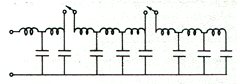
Type "E" Pulse Forming Networks are the most commonly used for all types of radar applications. By definitions, a type "E" network is defined as having equal capacitance per mesh and mutual inductance between adjacent coils.
The common practice for use of a type "E" network is indicated in the circuit Figure a.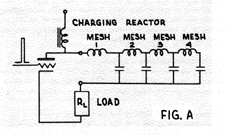
Activating the switch type discharge the energy of the capacitors through the inductors of the pulse forming network, resulting a flat topped wave across R¡. The squareness of the wave is entirely a function of the number of meshes provided the external circuit is non-reactive. In addition, the energy stored in the network will be completely dissipated into the load R¡ when it matches the characteristic impedance of the pulse forming network. Furthermore, the voltage appearing across the load is one-half the voltage at which the network is charged.
The number of MESHES or SECTIONS of a pulse forming network is determined by the rise time requirements and the duration of the pulse width. Basically, the rise time of the network is determined by the rise time of one mesh of the network. Shortening the pulse width of the mesh decreases the rise time. This results in the need for more meshes for a given pulse width. Total capacitance requirements of a type "E" pulse forming network
| C = T / 2Z |
| C = microfarads |
| T = time in microseconds |
| Z = characteristic impedance |
Capacitance per mesh is the total inductance divided by the number of meshes. Similarly, the total inductance is
|
L = TZ / 2
|
| L = inductance in microhenrys |
Inductance per mesh is the total inductance divided by the number of meshes.
From the practical standpoint, the first and last inductor are generally larger and the others are smaller. This, in conjunction with proper adjustment of the mutual between adjacent inductors, results in a flat topped discharge wave.
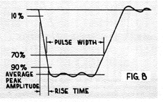 Rise Time requirements is determined from the magnetron characteristics in conjunction with the pulse transformer and other components in the modulator circuit. A long rise time will result in poor spectrum characteristics and a rise time which is too short might result in magnetron sparking, overshoots and other undesired characteristics of operation. For ease of specifying, rise time is generally indicated along the linear portion of the wave front and measured from 10% to 90% of the average peak amplitude. (See Figure b) Rise Time requirements is determined from the magnetron characteristics in conjunction with the pulse transformer and other components in the modulator circuit. A long rise time will result in poor spectrum characteristics and a rise time which is too short might result in magnetron sparking, overshoots and other undesired characteristics of operation. For ease of specifying, rise time is generally indicated along the linear portion of the wave front and measured from 10% to 90% of the average peak amplitude. (See Figure b)
| Case Base Dimensions |
K |
L |
G |
H |
J |
| A |
B |
Footed Bracket |
Spade Bracket |
Max |
Max |
| 1-3/4 |
1 |
2-1/2 |
2-1/16 |
3-1/16 |
25/32 |
* |
.213 |
| 2-1/2 |
1-3/16 |
3-1/4 |
2-3/4 |
3-13/16 |
29/32 |
* |
.213 |
| 3-3/4 |
1-1/4 |
4-7/16 |
4 |
5 |
29/32 |
* |
.213 |
| 3-3/4 |
1-3/4 |
4-7/16 |
4 |
5 |
1-1/2 |
5/8 |
.213 |
| 3-3/4 |
2-1/4 |
4-11/16 |
4 |
5-1/4 |
2 |
1-1/4 |
.213 |
| 3-3/4 |
3-3/16 |
4-11/16 |
4 |
5-1/4 |
2-7/8 |
2 |
.213 |
| 4-9/16 |
3-3/4 |
4-11/16 |
4 |
5-1/4 |
4-5/16 |
3-3/8 |
.213 |
| 6 |
4-11/16 |
5-11/16 |
N/A |
6-1/4 |
4-13/16 |
4-1/4 |
.213 |
| 7-3/8 |
5-5/8 |
6-1/2 |
N/A |
7-1/8 |
6-1/16 |
5-1/2 |
.213 |
| 8 |
4 |
10-1/8 |
N/A |
11-1/4 |
4-9/32 |
2-1/8 |
.437 |
| 13-1/2 |
4-1/8 |
15-5/8 |
N/A |
16-3/4 |
4-13/32 |
2-1/8 |
.437 |
| 13-1/2 |
5-1/8 |
15-5/8 |
N/A |
16-3/4 |
5-13/32 |
3-1/8 |
.437 |
* Single slot or lug centered-J Hole or slot diameter on footed brackets.
Brackets for base sizes 4-9/16 x 3-3/4, 6 x 4-11/16 and 7-3/8 x 5-5/8 are mounted on the side parallel to the centerline drawn through the terminal |
 Pulse Width is a requirement which is determined from various factors, such as range, of the radar system. Pulse width is ordinarily specified at 70% of the average peak amplitude (he half power point). Pulse width can be fixed accurately in the pulse forming network and remain stable for many years. Pulse Width is a requirement which is determined from various factors, such as range, of the radar system. Pulse width is ordinarily specified at 70% of the average peak amplitude (he half power point). Pulse width can be fixed accurately in the pulse forming network and remain stable for many years.
Many radar equipments require multiple pulse widths. This can be achieved in two ways, i.e., by the use of individual pulse forming networks in separate or one container. This, ordinarily, is space consuming upon considering the possibilities of the additive network. The figure illustrates a typical additive pulse forming network with the capability of supplying three pulse widths, each working into a nominal design impedance with the same rise time.
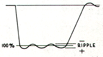 Ripple is defined as the voltage excursions above and below the average peak amplitude of the pulse feeding a non-reactive resistance load. Designing and manufacturing pulse forming networks with low ripple requires good basic coil design and close tolerance manufacturing. Ripple is defined as the voltage excursions above and below the average peak amplitude of the pulse feeding a non-reactive resistance load. Designing and manufacturing pulse forming networks with low ripple requires good basic coil design and close tolerance manufacturing.
Normal ripple tolerance of 5% for single networks or 7.5% for additive networks excursion from the average peak amplitude is relatively easy to obtain. This ripple percentage is suitable for many applications. However, it is possible to obtain ripple percentages of ±2% for single networks and ±4% for additive networks by closer adjustment of the network component parts.
The listing of two terminal pulse forming networks which follows is intended to give the engineer an insight into the effect of variable size and operation. It is especially interesting to note the effect of repetition rate with various types of capacitor dielectrics.
Temperature Range is indicated at the head of each listing. Please note column which indicates repetition rate for 10°C rise. The ambient temperature plus the internal heat rise should never exceed the maximum of the temperature range. The design repetition rate is based on still air operation. Example: Part # NH50-500 has an indicated temperature rise of 10°C for a repetition rate of 500 PPS. The heading indicates a maximum ambient temperature of 75°C. This means that at half power input, the ambient could be raised to 80°C, or if the repetition rate was doubled, resulting in a 20°C internal heat rise, the ambient must be lowered to 65°C.
Forced Air Cooling and/or the addition of cooling fins can increase the power dissipation of the container. This results in a lower internal heat rise for a given repetition rate or for an increased repetition rate for a given internal heat rise. The low ambient temperature indicates the lowest temperature at which the pulse forming network is guaranteed to work.
Decay or Fall Time is approximately three times the value of the rise time for a Type "E" pulse forming network.
Salt Spray: All listed pulse forming networks are designed to withstand a 50 hour salt spray test per MIL-Q-151A. 100 hour withstand is also available.
Humidity: Per paragraph 3.12 humidity cycle of MIL-C-25A or 30 day cycle per MIL-E-5272.
Vibration: Per MIL-C-25A, 10 to 55 cps for .060" total excursion traversed once per minute. One hour in each plane and using the mounting clamps as used in end equipment.
Temperature and Immersion Cycling: Per MIL-C-25A paragraph 4.6.9.
Life Test: The pulse forming networks are designed to withstand the following life test:
Impedance: The listed pulse forming networks are established for a matching impedance of 50 ohms ± 5 ohms into a resistive load. All other characteristic measurements are also made with a 50 ohm resistive load. Other impedance values are available. Since the impedance largely determines the size of the network for a given duration, a generality might be made whereby the following is substantially true. The cubical volume of a pulse forming network is inversely proportional to the matching impedance. This statement is made for the engineer who requires another matching impedance for the purpose of evaluating the approximate size.
NETWORKS NOT LISTED:
Additive Networks The engineers of Plastic capacitors, Inc. are prepared to design additive networks to your specification. High voltage networks with external coils for high power installations, while not commonplace, are being made regularly to specification. Current peaks of 4000 amperes and charging voltage of 80KV are readily achieved and are not the limit of practicability.
How to Specify The following information is required for the design of pulse forming networks.
| 1. Peak charging voltage. |
2. Pulse duration - where measured and tolerance. |
| 3. Pulse rise time - where measured and tolerance, if any. |
4. Characteristic impedance and tolerance. |
| 5. Repetition rate. |
6. Maximum ripple allowable. |
| 7. Temperature range - operational and storage. |
8. Operational life required. Describe fully. |
| 9. Decay or fall time, if pertinent. |
10. Vibration and shock requirements. |
| 11. Altitude of operation. If pressurized, so state. |
12. Forced or natural air circulation. |
| 13. Number of terminals required. |
14. Limiting dimensions. |
| 15. Mounting brackets required. |
16. Other environmental requirements. |
| 17. Other mechanical requirements such as weight, unusual configuration, etc. |
PULSE FORMING NETWORKS WITH PAPER CAPACITORS
CHARACTERISTIC IMPEDANCE 50 OHMS TEMPERATURE RANGE -40°C TO 55°C
|
1000 Peak Charging Volts
|
2000 Peak Charging Volts
|
| Part Number |
Micro Second Pulse |
PPS per 10°C Rise |
Case Dimensions |
|
Part Number |
Micro Second Pulse |
PPS per 10°C Rise |
Case Dimensions |
| A |
B |
C |
A |
B |
C |
|
NP 10-50
|
0.5 |
|
1-3/4 |
1 |
2-1/8 |
|
NP 20-50
|
0.5 |
2200 |
1-3/4 |
1 |
2-1/8 |
|
NP 10-100
|
1.0 |
5000 |
1-3/4 |
1 |
2-1/2 |
|
NP 20-100
|
1.0 |
2100 |
2-1/2 |
1-3/16 |
2-1/8 |
|
NP 10-200
|
2 |
4200 |
2-1/2 |
1-3/16 |
2-1/8 |
|
NP 20-200
|
2 |
1900 |
2-1/2 |
1-3/16 |
2-1/2 |
|
NP 10-400
|
4 |
2100 |
2-1/2 |
1-3/16 |
2-1/8 |
|
NP 20-400
|
4 |
700 |
2-1/2 |
1-3/16 |
3 |
|
NP 10-500
|
5 |
2200 |
2-1/2 |
1-3/16 |
3 |
|
NP 20-500
|
5 |
700 |
2-1/2 |
1-3/16 |
4 |
| 3000 Peak Charging Volts |
4000 Peak Charging Volts |
|
NP 30-25
|
0.25 |
4200 |
2-1/2 |
1-3/16 |
2-1/2 |
|
NP 40-25
|
0.25 |
2400 |
2-1/2 |
1-3/16 |
2-1/2 |
|
NP 30-50
|
0.5 |
2100 |
2-1/2 |
1-3/16 |
2-1/2 |
|
NP 40-50
|
0.5 |
1200 |
2-1/2 |
1-3/16 |
2-1/2 |
|
NP 30-100
|
1.0 |
1200 |
2-1/2 |
1-3/16 |
3 |
|
NP 40-100
|
1.0 |
700 |
2-1/2 |
1-3/16 |
3 |
|
NP 30-200
|
2 |
780 |
2-1/2 |
1-3/16 |
4 |
|
NP 40-200
|
2 |
440 |
2-1/2 |
1-3/16 |
4 |
|
NP 30-400
|
4 |
380 |
3-3/4 |
1-1/4 |
2-1/2 |
|
NP 40-400
|
4 |
240 |
3-3/4 |
1-1/4 |
3 |
|
NP 30-500
|
5 |
340 |
3-3/4 |
1-1/4 |
3 |
|
NP 40-500
|
5 |
220 |
3-3/4 |
1-1/4 |
3-1/2 |
| 5000 Peak Charging Volts |
7500 Peak Charging Volts |
|
NP 50-25
|
0.25 |
2100 |
2-1/2 |
1-3/16 |
3 |
|
NP 75-10
|
0.1 |
2300 |
2-1/2 |
1-3/16 |
3-1/2 |
|
NP 50-50
|
0.5 |
1000 |
2-1/2 |
1-3/16 |
3 |
|
NP 75-25
|
0.25 |
920 |
2-1/2 |
1-3/16 |
3-1/2 |
|
NP 50-75
|
0.75 |
700 |
2-1/2 |
1-3/16 |
3-1/2 |
|
NP 75-50
|
0.5 |
500 |
2-1/2 |
1-3/16 |
4 |
|
NP 50-100
|
1.0 |
500 |
2-1/2 |
1-3/16 |
3-1/2 |
|
NP 75-75
|
0.75 |
410 |
3-3/4 |
1-1/4 |
3-1/2 |
|
NP 50-200
|
2 |
335 |
2-1/2 |
1-3/16 |
5 |
|
NP 75-100
|
1.0 |
350 |
3-3/4 |
1-1/4 |
4 |
|
NP 50-400
|
4 |
200 |
3-3/4 |
1-1/4 |
3-1/2 |
|
NP 75-200
|
2 |
230 |
3-3/4 |
1-3/4 |
4-1/2 |
|
NP 50-500
|
5 |
200 |
3-3/4 |
1-3/4 |
4-1/2 |
|
NP 75-400
|
4 |
150 |
3-3/4 |
2-1/4 |
5-1/2 |
| |
|
|
|
|
|
|
NP 75-500
|
5 |
140 |
3-3/4 |
3-3/16 |
5-1/2 |
| 10,000 Peak Charging Volts |
15,000 Peak Charging Volts |
|
NP 100-10
|
0.1 |
1900 |
3-3/4 |
1-3/4 |
3-1/4 |
|
NP 150-10
|
0.1 |
900 |
3-3/4 |
1-3/4 |
4-1/2 |
|
NP 100-25
|
0.25 |
760 |
3-3/4 |
1-3/4 |
3-1/4 |
|
NP 150-25
|
0.25 |
430 |
3-3/4 |
1-3/4 |
5 |
|
NP 100-50
|
0.5 |
430 |
3-3/4 |
1-3/4 |
3-3/4 |
|
NP 150-50
|
|
|
|